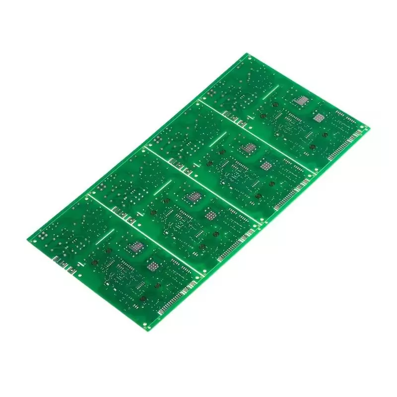
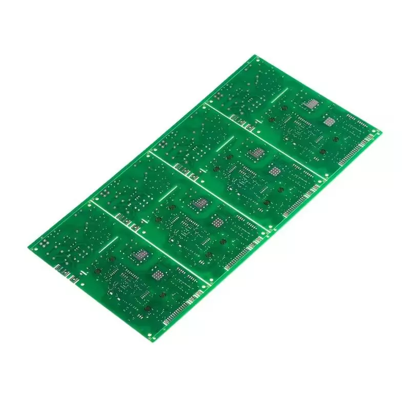
Green Solder Mask PCB
Hoshineo Lcd-Tech Factory provides various series of Green Solder Mask PCB (Printed Circuit Board, printed circuit board) is a key component in electronic equipment, used for mechanical support and electrical connection of various electronic components. PCB board has high quality and suitable price, exported to Europe, America and Southeast Asian countries.
Send Inquiry
Product Description
Green Solder Mask PCB provided by Hoshineo Lcd-Tech refers to the PCB coated with a layer of green solder resistance substance on the non-wired area of the PCB. The main function of this green solder resistance layer is to prevent the flow of solder at high temperature during the welding process from affecting the area that does not need to be welded, ensuring the accuracy of welding and the reliability of the circuit board.
Hoshineo Lcd-Tech Green Solder Mask PCB product parameters:
|
Place of Origin: |
zhejiang, China |
|
Base Material: |
FR4 |
|
Layer: |
1-64 Layers |
|
Copper Thickness: |
1oz |
|
Board Thickness: |
1.6mm |
|
Min. Hole Size: |
0.15mm |
|
Min. Line Width: |
3 Mil |
|
Min. Drilling: |
0.1mm |
|
Surface Finishing: |
HASL, Immersion gold(ENIG), OSP |
|
Solder Mask Color: |
Green, White, Black, Red, Blue, Etc. |
|
Silkscreen Color: |
White, Black, Etc. |
Hoshineo Lcd-Tech Green Solder Mask PCB Features and functions
Solder stop function: TheGreen Solder Mask PCB can effectively prevent the solder from flowing to the area that does not need to be welded during the welding process, and protect the lines and components on the circuit board.
Insulation protection: The green solder shield acts as an insulating protection to prevent short circuits between the lines on the circuit board.
Manufacturability and aesthetics: The green solder resistance layer makes it easier to carry out plugins and subsequent repairs during the manufacturing process, while improving the aesthetics of the board.
Hoshineo Lcd-Tech Green Solder Mask PCB Details
Packaging&shipping
To better ensure the safety of your goods, professional, environmentally friendly, convenient and efficient packaging services will be provided.
FAQ
Q:What payment do you accept?
A:T/T, L/C, Western Union, PayPal, Ali Pay, Credit Card
Q:Which countries have you worked with?
A:US, Canada, Italy, Germany, Czech Republic, Australia, Japan, and so on.
Q: What is your Lead time?
A:Lead time is usually punctual here, usually 5-10 days for PCB sample, 10-15 days for mass production.
For some special situation, we can also advise customer in advance to avoid any in expectation or loss at customer side.
Q:What is your package?
A:With Inner vacuum package and outer carton.
Related Category
Send Inquiry
Please feel free to give your inquiry in the form below. We will reply you in 24 hours.