This guide will help you quickly understand PCB boards.
A PCB, also known as a circuit board, is an important electronic component.
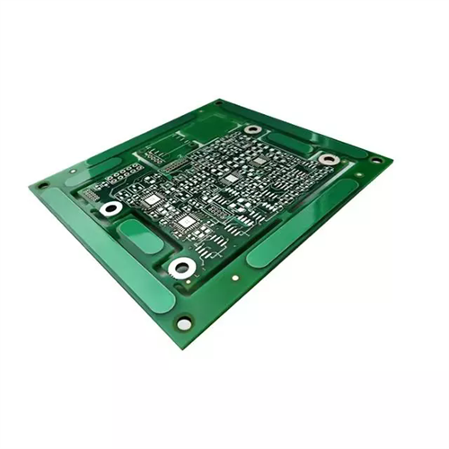
1. Traditional circuit boards are made by printing the circuit diagram and layout using a photoresist method, hence the name printed circuit board. Currently, most circuit boards are coated with an attached photoresist (laminate or coating), which is then exposed and developed before the circuit board can be etched.
2. Circuit boards are classified into single-sided, double-sided, and multi-layer boards. On the most basic PCB, components are concentrated on one side, and the wires are concentrated on the other side; this type of PCB is called a single-sided board. A double-sided board has copper traces on both sides, and the lines between the two layers can be connected through vias to form the required network connection. A multi-layer board refers to a printed circuit board with three or more conductive pattern layers separated by insulating materials and laminated together, with the conductive patterns interconnected as required.
3. A circuit board mainly consists of solder pads, vias, mounting holes, wires, components, connectors, fillers, and electrical boundaries. The main functions of each component are as follows:
| 1 |
Pad |
Metal holes used for soldering components |
| 2 |
Through Hole |
Including metal through holes and non-metal through holes; metal through holes are used to connect pins between components of each layer |
| 3 |
Mounting Hole |
Used for fixing the circuit board |
| 4 |
Conductor |
Copper film network used for connecting component pins |
| 5 |
Connector |
Used for connecting components between circuit boards |
| 6 |
Filler |
Applying copper wire to the ground network can effectively reduce impedance |
| 7 |
Electrical Boundary |
Used for determining the size of the circuit board |